
EMI Filter Insertion Loss Explained: Why Off-the-Shelf Filters Fail in Variable Speed Drives
- Jan 30
- 7 min read
Updated: Feb 4
EMI filter insertion loss is often treated as a simple datasheet parameter, but in real power electronics systems it depends strongly on source and load impedance. This is why off-the-shelf EMI filters frequently underperform—or even make EMC problems worse—in variable speed drives and AC-powered converters
At the end of January, I had the pleasure of spending a day back at my old School of Engineering at Newcastle University (formerly the School of Electrical and Electronic Engineering, before it was merged with other engineering departments). I was there as an external examiner for an industrial PhD thesis. It brought back a lot of memories—particularly of sitting nervously in a small room 14 years ago, preparing for my own viva. Time really does fly.
That experience prompted me to start writing a series of technical articles on EMC design topics. This is the first of those articles. Here, I want to discuss filter insertion loss, and more importantly, why engineers often find that off-the-shelf filters do not deliver the expected performance once installed in real systems. I will also include some practical case studies later in the article.
Basics of Insertion Loss
To understand the insertion loss of a filter, it is essential to recognise that filter performance depends strongly on both the noise source impedance and the load impedance. This applies to both differential-mode and common-mode noise paths. A simplified representation is shown in the diagram below.

The following simulation demonstrates how variations in source and load impedance can significantly affect the measured insertion loss of a filter. Four source-load scenarios are simulated. It can be seen that each scenario results in a different insertion loss. It is also worth highlighting that accurately simulating real filter performance is not trivial. Even in a relatively simple simulation set-up, factors such as coupling within the common-mode choke, parasitic elements of inductors and capacitors, and any damping components all need to be considered to obtain meaningful results.

The example shown here focuses only on the differential-mode performance of the filter. It also illustrates how insertion loss is calculated in practice: a fixed-amplitude noise source is applied (in this case, 1 V peak-to-peak), a frequency sweep is performed while keeping the source amplitude constant, and the resulting voltage across the load is measured. The insertion loss is then calculated as:
Insertion Loss = 20 log(V₂ / V₁)
Where V2 is the voltage measured on the load with a filter and V1 is the voltage measured on the load without a filter.
Source and Load Impedances for Power Electronics Applications
This naturally leads to the next question: how do we know the source and load impedances?The honest answer is that, in most cases, we don’t—at least not precisely. Different circuits and products can exhibit very different impedance characteristics. That said, there are some rules of thumb we can rely on, particularly if you are working with variable speed drives or designing filters for switched-mode power supplies, such as DC-DC converters.
As always, any discussion of noise must start with a clear separation between differential mode and common mode. We will begin with differential mode.
The diagram below shows the differential-mode output impedance characteristics of a DC-DC converter. It can be seen that across some defined frequency range, the output impedance of the converter is extremely low. This is exactly what we would expect: a high output impedance would imply higher losses (I²R), so switched-mode power supplies are typically designed to have very low output impedance. This is often achieved with good output capacitor selections and layout. But beyond certain frequency, it is expected that the impedance will increase (when the ESL of capacitors start to take effect).
But the input impedance of a switched-mode power supply is a much more complicated story. It depends on several factors:
For AC-powered mains products, whether a PFC circuit is involved.PFC forces the input current to be in phase with the mains voltage. To achieve this, the control feedback must be sufficiently slow, which results in an increased input impedance starting from relatively low frequencies.
The EMI filter design at the front end. Within certain frequency ranges, the input impedance is dominated by high-impedance components, particularly inductors.
The control algorithm and several other secondary factors.
As a result, the differential-mode input impedance of a switched-mode power supply is complex and highly frequency dependent. In practice, it is often relatively high in the frequency range where EMC conducted emission tests begin (9 kHz or 150 kHz). For reference, we previously showed the input impedance of a three-phase voltage source inverter; note that in this case the impedance is expressed in dBΩ.

So far, the discussion has focused mainly on differential mode. For common mode, the situation is conceptually simpler but practically more challenging. Ideally, we want a very high common-mode impedance, because for a given common-mode voltage this would result in a smaller common-mode current. However, achieving this in real systems is extremely difficult due to unavoidable parasitic capacitances between the power supply and earth or chassis.
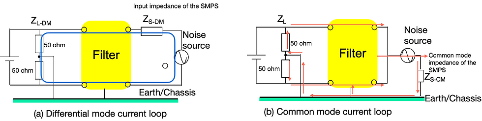
When testing products such as switched-mode power supplies or motor drives, a LISN is used. From a differential-mode perspective, the simplified diagram below illustrates the effective load impedance. In this case, the load impedance is defined by the LISN itself, since the noise source originates within the switched-mode power supply.
From a differential-mode point of view, the LISN can be treated as having an impedance of roughly 100 Ω (two 50 Ω in series). If we now think about filter insertion loss, a more realistic impedance model would therefore be a varying source impedance feeding into a 100 Ω load impedance. This is quite different from what is commonly assumed in filter datasheets (50 Ω - 50 Ω).
So far, this discussion is purely in differential mode. For common mode, the common mode source impedance depends heavily on how the product is grounded or earthed. Is the product floating with respect to ground, or is it bonded to chassis? If it is bonded, how long is the bonding strap or connection? All of these factors directly affect the common-mode source impedance. And, impedance always varies with frequency.
However, on the load side, the EMC test setup is much more clearly defined. As shown in the diagram below, the common-mode load impedance in a typical LISN-based setup can be simplified to 25 Ω (two 50 Ω in parallel).
Now, let us look at a typical filter manufacturer’s datasheet. In most cases, the insertion loss is specified with both the source and load impedances defined as 50 Ω / 50 Ω. The manufacture often tests both differential mode (symmetrical) and common mode (asymmetrical). This naturally raises a question: given that these filters are almost always used to suppress mains noise generated by power supplies, why is a 50 Ω / 50 Ω system used at all?

A very good question indeed. If we dig into the history, and look at older datasheets (see the diagram below from Schaffner, now TE), you will notice that there are actually four different insertion-loss curves shown. The extra two curves are perhaps much more useful. So times have clearly changed, and it seems we have lost some of the “good stuff”.

I can, however, understand why manufacturers have moved toward publishing only 50 Ω / 50 Ω measurements.
First, the measurement itself is simple and straightforward. A VNA or impedance analyser inherently has a 50 Ω source and a 50 Ω load, so the test can be completed very quickly and repeatably.
Second, even if manufacturers invested additional time and resources to characterise filters under different source and load impedances, the reality is that very few customers would use or even understand that information. Several manufacturers have told me that around 95% of customers who buy these filters would not know how to interpret the additional curves. Unfortunately, this aligns well with what I have seen in the field.
So, whether we like it or not, this is the reality we are working with today.
Insertion Gain
Another important issue, in my opinion, is that if you look at the diagram above, in the lower frequency range, there is actually an insertion gain rather than an insertion loss. This behaviour is caused by resonance within the filter circuit itself.
Under the 50 Ω / 50 Ω condition, this insertion gain is not particularly obvious. However, if you examine the other two load conditions, the resonance shifts to below 100 kHz and the magnitude of the insertion gain becomes significantly worse.
The following case study illustrates this issue.
A variable speed drive manufacturer recently encountered an issue when using a third-party EMI filter between the drive and the load. They observed significantly high common-mode current circulating between the unit and the protective earth. It is worth noting that this is a megawatt-level converter, so excessive low-frequency common-mode current becomes a serious concern.
Further investigation showed that the dominant common-mode noise frequency was approximately the third of the IGBT switching frequency, at around 48 kHz. This left the engineering team puzzled, as the EMI filter appeared to exacerbate the problem rather than mitigate it.
After reviewing the filter manufacturer’s datasheet, a clear conclusion could be drawn. At 48 kHz, the filter exhibits an insertion gain rather than an insertion loss under realistic operating conditions. Because the manufacturer only provides insertion-loss data under a 50 Ω / 50 Ω condition, this behaviour is not obvious in the datasheet. Under that test condition, the common-mode insertion gain at 48 kHz appears to be close to 0 dB.
However, as shown in the diagram above, when the filter is tested under different source and load impedances, the resonance point shifts to a lower frequency and moves clearly into the insertion-gain region. This explains why, in the real system, the filter amplified the common-mode noise instead of attenuating it.
From this, we can conclude that the root cause of the issue lies in the impedance mismatch between the real system and the filter characterisation conditions used in the datasheet.
Installation & Layout
Lastly, filter performance—particularly in common mode—depends heavily on the quality of the earthing connections. A short, direct, and low-impedance connection to earth or chassis is absolutely essential to achieve the intended filter performance.


Comments